Technology of sedimentation from solutions of conducting patterns on photochemically activated polymeric substrates
 Purpose
Selective sedimentation from solutions of conducting patterns from copper, nickel and other metals on dielectric surfaces, not containing metal foil, without using photolithography operations.
Characteristics
Technological characteristics:
- The composition of the dielectric substrate polyimide, polyethylene terephthalate, polyamide, glassceramics, etc.
- The composition of conducting metal - copper, nickel.
- The set thickness of conductors is provided with chemical sedimentation from solutions of copper or nickel (up to 0,2 microns) and the subsequent electrochemical sedimentation of copper (till 25-35 a micron) or chemical sedimentation of nickel (up to 12 microns).
- There is an opportunity for subsequent sedimentation of other metals and alloys (for example gold, alloy Sn-Pb).
- The minimal sizes of elements at thickness of conductors of 0,2-5 microns are 10-20 microns, and at thickness of 10-25 microns can be up to 40-100 microns.
- The minimal diameter of metallized apertures at thickness of dielectric 40 microns are 40 microns.
- Adhesive durability of ''conducting element'' system - substrate 500-800 Н/м.
- Resistance of isolation is determined by the composition of dielectric (if polyimide is used it is 10 exp. 4 MOhm).
- Number of flexible substrate kinks (polyimide) up to bursting of copper conductors (at diameter of a kink of 6 mm) - 6000.
Advantages of technology:
- Significant reduction of labor and material expenses (twice in comparison with half-additive way of printed-circuit-boards manufacture).
- Variation of composition of sedimented metal (copper, nickel, tin, gold, etc.).
- Variation of thickness of coatings within the limits of 0,1-35 microns and more.
- Manufacturing conducting elements of small sizes, starting from 10 microns.
- Manufacturing elements not connected to each other in a closed circuit.
- Use of nonfoil-clad dielectrics of different chemical composition.
Application
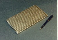
Manufacture of rigid and flexible printed-circuit-boards and cables on thermostable substrate, multilayered printed-circuit-boards with high density of installation, wave guides, heating elements for irons, washing machines, windscreens of automobiles, etc.
Condition of production
Made to order
Maintenance documents
Technological documentation

